CHIP-8 in hardware - part 1 (ALU)
Implementing CHIP-8 in hardware, part 1
I got into FPGAs with the intent of building a retro-computer. A couple of popular hardware implementation targets are Gameboy, NES, RISC-V and CHIP-8. Last year I’ve done my practice round with 6502 and RISC-V emulators, both in C.
CHIP-8 is a really nice virtual machine implemented on a number of computers since the 1970s, initially designed to make game development easier.
After building a CHIP-8 emulator/interpreter (TODO link) a couple of days ago I thought I know a lot about the simple platform to actualy start implementing it in hardware, in Verilog and deploy to an FPGA board.
Why do it in hardware?
Because it is fun! CHIP-8 seems much simpler than other platforms, as it was interpreted on 1970s hardware, so I think I could finish this project in a couple of afternoons.
The target platform
I’m developing and testing against an Altera Cyclone IV development board, with two video outputs - 128x64 LCD display, VGA output. The board also features a buzzer for sound output. A 4x4 matrix keypad will serve as an input device.
High-level design
I have some components already left over from my previous FPGA projects - such as a keypad controller and a memory-mapped display.
I plan to map the 64x32 pixels into the framebuffer/display RAM and let the existing pixel generator render it on an LCD/VGA external display, scaling the CHIP-8 pixels into larger squares.
It’s probably too early to finalize the entire design, but I think it will consist of these parts:
- CPU
- RAM
- keypad controller
- display RAM
- display controller
- buzzer controller
- pseudorandom generator
- top module to wire them together
CHIP-8 Virtual machine description:
CHIP-8 is a really simple platform, should be well within the capabilities of a cheap modern FPGA.
- 64x32 pixel monochrome display
- 4K of 8-bit RAM
- 16 8-bit “variable” registers V0-VF
- I 16-bit address register
- Stack of 16-bit addresses for call/return
- 16-bit PC - program counter
- 8-bit delay timer (decremented at 60 Hz) until it reaches 0
- 8-bit sound timer (decremented at 60 Hz), beeps when it reaches 0
- 16- key keypad that sends scan codes 0x1-0xF
ROMs
ROMs will be “compiled” into the RAM initialization file for the time being - at least in the initial stages I’ll use a Python tool to prepare the entire RAM image with the font and game ROM located at their respective addresses.
CHIP-8 CPU roadmap
In my reference implementation in C the fetch/decode/execute loop was handled by a single function that:
- read the instruction bytes from the memory
- used a giant nested switch statement to implement the individual opcodes
Managing the complexity is key in hardware design, so I’ll try to break the giant switch into several modules that can be developed and tested independendly.
We can handle the fetch part trivially, reaching into the RAM and reading two bytes in two clock cycles.
An instruction decoder can help with the decode part of execution, trying to extract as much information from the opcode as possible.
We can offload the 8XYN instruction an an ALU as the arithmetic 8XYN instructions were dispatched to the 1802’s ALU, so we can start by implementing a similar ALU.
I suspect I might also end up with a blitter module that will handle the DXYN drawing opcode.
Execution and clock cycles
I think that many of the opcodes will be able to execute in a single clock cycle.
The most complex opcode is the DXYN one that draws a sprite at XY coordinate, as this will definitely take several clock cycles.
There are several other suspicious opcodes that could take more clock cycles - 00E0 clear screen, FX33 BCD operation, FX55 and FX65 for register store / load.
Part 1: ALU
CHIP-8 was originally designed for the RCA 1802 microprocessor. The arithmetic 8XYN instructions were dispatched to the 1802’s ALU, so we can start by implementing a similar ALU.
The C implementation in emuchip8 was procedural, so it doesn’t translate well into circuits and it can be implemented in pure combinational logic.
Two of the nine CHIP-8 “ALU opcodes” are vx-vy and vy-vx. We can implement both in a single ALU subtract operation and swap the inputs.
ALU opcodes
| op | result | |
|---|---|---|
| 0 | y | |
| 1 | x | y |
| 2 | x&y | |
| 3 | x^y | |
| 4 | x+y with carry | |
| 5 | x-y with borrow | |
| 6 | x»1 | |
| 7 | x«1 |
ALU in Excel
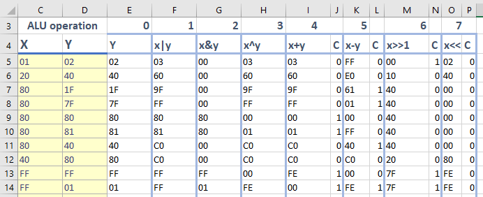
To prepare test data I’ve used trusty Excel, where I encoded the ALU operations with mostly various edge case inputs I thought could cause trouble with wraparound.

ALU operations with inputs, outputs and carry flag
ALU in Verilog
I’ve made use of Verilog headers, which keep common constants. These headers get included into the ALU (and later in the instruction decoder) modules.
Then we use straightforward combinational logic to implement every ALU operation - as seen in the code.
Validating with a test bench
I’ve generated a simple test bench that iterates over X,Y inputs and combines them with every operation (0-7).

What’s next?
Instruction decoder that will break down the CHIP-8 opcodes into ALU operations.