Adventures in hardware, part 2 - even lower level
I’ve went through the first part of From Nand to Tetris course where I learnt to build a simple 16-bit computer called Hack from the digital building blocks (NAND gates). The course used its specific HDL (hardware definition language), which is a gentle way to shield a beginner from the ugliness of a real language, but to implement anything on a real FPGA board one needs to use VHDL or Verilog. (Or a higher-level hardware definition language like Chisel or JHDL.)
Hello FPGAs
We usually develop software by writing code that gets compiled to instructions running on a general-purpose CPU (or a GPU). Another route is by designing a special circuit for the specific project. FPGA (Field-programmable gate array) is a device that can be configured to implement this design.
In comparison to usual integrated circuits, FPGAs can be reprogrammed and some can also be dynamically reconfigured during runtime to match a specific workload (imagine your CPU growing an accelerator chip for data processing, compression or encryption). They are also much cheaper to program, as prices of fabricating a chip are not for the faint of heart.
A microcontroller or a CPU executes 1 instruction at a time (or more if it has multiple cores), while circuits and FPGAs can be massively parallel as they can process inputs, perform combination logic, remember stuff and generate output every clock cycle.
They are also much harder to program with a completely different tooling to one I’m used to, harder to debug, and with incredibly long compile times.
My FPGA
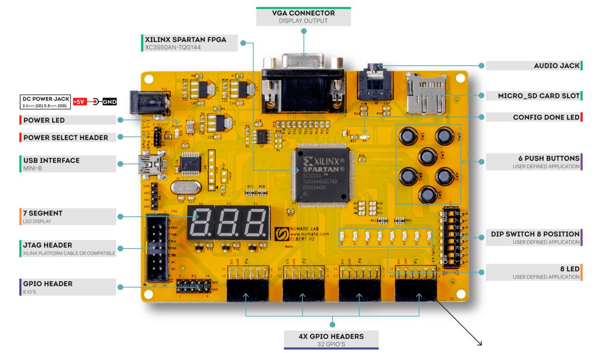
I’ve dusted off my old Elbert v2 FPGA development board, which has a Xilinx Spartan XC3S50A chip. To interact with the logic one can either use a handful of “primitive” IOs - such as 8 LEDs, 6 push buttons and 8-contact DIP switch, a higher-level 7-segment LED display or VGA and audio output. There are also 39 IO pins to connect other peripherals. It was the cheapest development board with some peripherals on board I could buy a year ago, so it’s definitely not state of the art.
Actual Hello World development
The IDE
The manufacturer recommends using Xilinx ISE 14.7 development environment. It’s a hefty 16.7 GB installation on my machine.
A joke says that Xilinx and Altera aren’t chip companies, they are primarily CAD software companies that also make FPGAs.
It’s quite ugly.
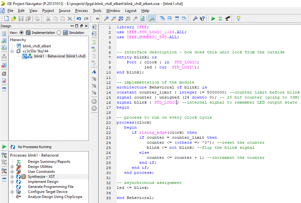
Blinking a LED in VHDL
We would like to blink a LED. Let’s start by creating an interface description of the blink1 module:
library IEEE; --libraries for the common data types
use IEEE.STD_LOGIC_1164.ALL;
use IEEE.NUMERIC_STD.ALL;

-- interface description - how does this unit look from the outside
entity blink1 is
    Port ( clock : in  STD_LOGIC;
           led : out  STD_LOGIC);
end blink1;
Next we start describing the implementation. First we need to define the internal signals and counters that we’ll use.
architecture Behavioral of blink1 is
constant counter_limit : integer := 6000000; --counter limit before blink
signal counter : unsigned (24 downto 0); -- 25 bit counter (going to 33M)
signal blink : std_logic; --internal signal to remember LED output state
begin
We want the LED to blink once per second. That means it should spend the first half of a second on and another half off. As we’ll later specify a 12 MHz clock signal, the counter_limit value is half of that (6 million). Because we will increment the counter every clock cycle, it will reach 6 million in 0.5 seconds, flip the output to on, reach another 6 million in another 0.5 seconds and flip the output to off and so on.
That means the process that we want to run on every clock cycle looks as follows, in pseudocode:
for(;;){
    if(counter == counter_limit){
        blink = !blink;
        counter = 0;
    else {
        counter++;
    }
    led = blink;
}
The same in VHDL:
-- process to run on every clock cycle
process(clock)
	begin
		if rising_edge(clock) then
			if counter = counter_limit then
				counter <= (others => '0'); --reset all bits of the counter to 0
				blink <= not blink; --flip the blink signal
			else
				counter <= counter + 1; --increment the counter
			end if;
		end if;
	end process;

-- asynchronous assignment
led <= blink;

end Behavioral;
Then we need to specify constraints for the Elbert v2 board based on the vendor-supplied UCF file to match the ports we defined for the blink1 entity. The UCF file describes how the pins on the board are physically connected to one of the 144 pins of the Spartan XC3S50A chip:
  NET "clock" LOC = P129  | IOSTANDARD = LVCMOS33 | PERIOD = 12MHz;
  NET "led"   LOC = P46  | IOSTANDARD = LVCMOS33 | SLEW = SLOW | DRIVE = 12;
Now we can “compile” the design - synthesize, map, place and route to end up with a bitstream - bits that describe the new internal logic of the FPGA chip. Building the programming file of this simple blinking hardware for the took 50 seconds on my developer machine.
Then we use the vendor-supplied configuration program to flash the blink1.bit
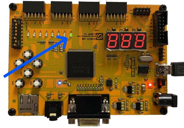
After uploading the bitstream to the board, it blinks! (the rightmost LED)
Adding a second module
Let’s also control a second LED by pushing a button:
We can implement this in another VHDL module where we just assign whatever signal button0 sends to led1:
library IEEE;
use IEEE.STD_LOGIC_1164.ALL;

entity blink_button is
    Port ( clock : in  STD_LOGIC;
           button : in  STD_LOGIC;
           led : out  STD_LOGIC);
end blink_button;

architecture Behavioral of blink_button is
begin
led <= button;
end Behavioral;
Note that the led port name is the same as on the previous module - it’s the
Well we might as well use this module more than once - let’s try connecting three buttons to two other LEDs, so that LED 1 will be toggled by button 0 and LED 2 by (button1 and button2).
Composing modules
To do this, let’s define a top module. This would be similar to the “main” entry point of a program. It will include all of the inputs and outputs and wire them to the child modules.
entity top_module is
    Port ( clock : in  STD_LOGIC;
	 LED      : OUT STD_LOGIC_VECTOR(2 downto 0);
	 Switch   : IN STD_LOGIC_VECTOR(2 downto 0)
	 );
end top_module;
Here it makes more sense to start using STD_LOGIC_VECTOR buses (logical grouping of signals). As there are 3 LEDs, we have defined LED bus of 3 signals as STD_LOGIC_VECTOR(2 downto 0);
Then in the implementation we first need to declare which components we’ll be working with (similar to including header files for C++ classes):
architecture Behavioral of top_module is

	COMPONENT blink1
	PORT(
		clock : IN std_logic;
		led : OUT std_logic
		);
	END COMPONENT;

	COMPONENT blink_button
	PORT(
		clock : IN std_logic;
		button : IN std_logic;
		led : OUT std_logic
		);
	END COMPONENT;

	signal button1and2 : STD_LOGIC;
And finally instantiate and wire the components. Please note that the switches on Elbert2 emit 1 if not pressed and 0 on pressed, so I invert the signal with the not operator. To combine signals from buttons 1 and 2 I’ve created a signal button1and2.
begin
	Inst_blink1: blink1 PORT MAP(
		clock => clock,
		led => LED(0)
	);

	Inst_blink_button1: blink_button PORT MAP(
		clock => clock,
		button => not Switch(0),
		led => LED(1)
	);

	Inst_blink_button2: blink_button PORT MAP(
		clock => clock,
		button => button1and2,
		led => LED(2)
	);

	button1and2 <= Switch(1) nor Switch(2);

end Behavioral;
Note: The instantiation templates can be obtained by clicking Design Utilities -> View HDL instantiation template in Xilinx ISE Design toolbox.
We also have to correspondingly update the UCF file with the mappings for LED and Switch pins.
The source
See the full source on GitHub.