Adventures in hardware, part 9 - FPGA calculator
A pocket calculator on FPGA
One potato two potatoes
Three potatoes, four!
Five potatoes, six potatoes
Seven potatoes, more!
As a follow up to one of my first FPGA projects Adventures in hardware, part 3 - display and a calculator I wanted to implement a more useful calculator that behaves like the common pocket calculators - you enter a number, choose an operator, enter another number, press another operator or = and see the result.
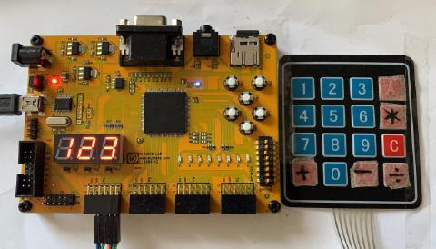
As my board only features three digit display, it will be slightly impractical and work on numbers from 0 to 999, but this time I wanted to operate it through a 4x4 keypad.
I’ve been stuck on how to properly read the keypad for quite some time - this was planned to be titled Hardware Adventures 5, not 9, after all.

I had to relabel some keys with a surgical tape and a marker.
The calculator architecture
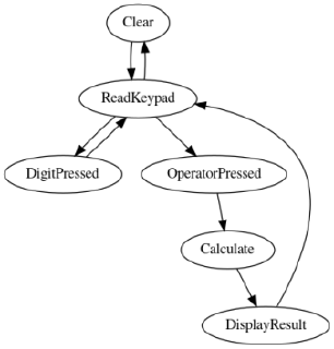
The main calculator logic is implemented by a state machine with a few registers:
RESULTholding the intermediate resultARGholding the currentlyDISPLAYholding whatever needs to be displayed on the LCD screenOPERATORholding the previously entered operator (+-*/)

A simplified calculator state machine
Notes on state transitions and register updates:
- When a digit gets pressed,
ARG <= ARG * 10 + digit - When an operator gets pressed,
OPERATORbecomes one of+-*/ - on
Calculatestate:RESULT <= RESULT OPERATOR ARGOPERATOR <= OPERATOR_NEXT
DISPLAYregister gets updated as required after states display_result and digit_pressed
Required modules
To support the main state machine work we’ll need several other components:
- keypad poller to debounce the keys
- keypad encoder to encode the keypad readout into a scancode
- binary to bcd encoder to convert the internal binary representation for display
- seven segment encoder to encode a BCD digit to segments
- seven segment driver to multiplex the three decimal digits over the shared wires
- integer divider to implement division
Reading a keypad
In a 4x4 matrix keypad the key switches are connected by a grid of wires arranged in 4 columns and 4 rows. To determine what button is pressed, we need to scanning the crossings of the rows and columns by activating each column one at a time and read back the status of the rows. There are several articles that elaborate on this topic, if you’re interested.
Using this information we can write a module that encodes a set of 4-bit row and column pins into a hexadecimal keycode.
Keypad layout:
 1 2 3 A
 4 5 6 B
 7 8 9 C
 * 0 # D
I decided to encode the * and # keys as 0xE and 0xF.
As I wanted to use this for a calculator, I’ve repurposed the C key for “Clear”, then applied a surgical tape to label the +-*/ keys.
We also need to enable builtin pull-down resistors on the row pins in order to ensure a known state (logical zero) when a button is not pressed instead of a floating input.
Entering multiple digits and displaying the number
Let’s represent the number internally as binary and just convert to the display using a BCD encoder.
The reading of the keys will be handled by the calculator state machine within its state_read_digit and state_digit_pressed states.
We can limit reading numbers larger than 999 by using a simple condition in the state_digit_pressed state:
if(reg_arg < 16'd100)
begin
    reg_arg <= reg_arg * 10 + keypad_out;
end
To display the DISPLAY register we initially convert the 10-digit number to BCD, then encode
each digit (ones, tens, hundreds) into bits for the seven-segment display and finally multiplex
them to the display.
A common algorithm for binary to BCD conversion is Double dabble and I’ve adapted a Verilog single-clock implementation into a 10-bit version .
Reading the keypad
Although I’ve found multiple descriptions for a single button debouncer, I didn’t understand how to do it over multiple possible columns that we scan and I attempted to insert some kind of debounce circuit running at a lower frequency after the keypad decoder, hoping it would settle on a decoded number - somehow it didn’t.
What finally helped was this assignment from a Tampere University that described the key poller and debouncer for the students. It describes an algorithm that probes the column successively, and for each column it waits for an input.
I could make the wait and hold times configurable, so it can be tuned to a specific keypad.
Decoding the keypad
This is quite straightforward Verilog
implementation, with nested case statements, that produces a 4-bit hex scancode for every row/column combination.
The calculator state machine
Now we just need to implement the top module implementing the state machine mentioned earlier in the article and connecting all the other modules.
Adding, subtracting and multiplying
We can implement the basic operations using straightforward Verilog, which will get synthesized into adders and a hardware multiplier, therefore implementing the operations in a single clock cycle.
if(reg_operator == OP_PLUS) begin
    reg_result <= reg_result + reg_arg;
    state <= state_display_result;
end else if(reg_operator == OP_MINUS) begin
    reg_result <= reg_result - reg_arg;
    state <= state_display_result;
end else if(reg_operator == OP_MULTIPLY) begin
    reg_result <= reg_result * reg_arg;
    state <= state_display_result;
Division
My FPGA tools won’t synthesize
the / operator, as a single-clock division by a variable number would be impractical to implement. I needed to implement a division module and wire it into the project.
The simplest algorithm of all is division by repeated subtraction :
while N = D do
  N := N - D
  Q := Q + 1
end
R := N
return (Q,R)
This translates to a straightforward Verilog implementation .
Integrating the divider module
As the division will run for a various number of clocks, we need to signal the parent module somehow that the division is completed:
We assign the divider inputs, signal it to start and transition into a waiting state:
end else begin //OP_DIVIDE
	divider_start <= 1'b1;
	numerator <= reg_result;
	denominator <= reg_arg;
	state <= state_dividing;
end
Then we continuously poll the done signal. If it’s asserted, we move over to the common display result state.
state_dividing:
begin
    divider_start <= 1'b0;
    if(divider_done)
    begin
        reg_result <= quotient;
        state <= state_display_result;
    end
end
In the real world one would probably use Long division as it’s completes in much less clock cycles than a simplistic division by subtraction.
Stupid errors I made along the way
-
I forgot again to connect a top module input to a pin. This will produce a cryptic message in Xilinx ISE and took some time to hunt down.
-
An earlier iteration of the keypad decoder couldn’t distinguish zero from a non-key press. I had to add
key_pressedsignal. -
Xilinx ISE doesn’t tell you when you make a typo in wire name, when you wire a module to something that doesn’t exist, for example
IO_P4_ROWasIO_DP4_ROW. -
An earlier iteration of the keypad scanner used a clock that was driven by a counter. This is considered a very bad practice and can result in glitches , results in creating new clock domains (which I don’t really understand yet). The solution is to run the slow logic on the same (fast) clock as everything else, but use a slow enable signal or use a PLL circuitry for clock division.