CHIP-8 in hardware - part 2 (CPU)
Continuing with the implementation of CHIP-8 in Verilog, I wanted to continue with the CPU module and get it to actually execute some instructions, so we’ll build an instruction decoder, CPU states and a register file.
As described in the previous part , we would like to:
- fetch instruction (2 bytes) from the memory into an 16-bit
opcoderegister - decode the instruction
- execute the instruction
Other articles in the series:
CPU opcodes
I can now divide the CPU opcodes into two groups - single-cycle simple operations and those that would require multiple clock cycles to execute.
Multi-clock cycle operations:
- 00E0 (clear screen)
- DXYN (draw)
- FX33 (binary to BCD)
- FX55 (dump registers V0 to Vx - needs multiple memory stores)
- FX65 (load registers V0 to Vx - needs multiple memory loads)
Single-clock operations are probably all the others.
The multi-clock operations would require additional state on the state machine that the execute state will transition to.
Some operations need to write back the value to the Vx (or V0) registers, so
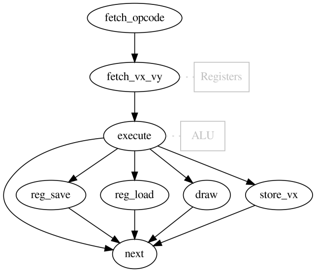
We can start enhancing the CPU state machine by adding the corresponding states (simplified):

In the current implementation, VY and VY are requested in parallel with the opcode, as we know the X and Y index from the first and second bytes.
This somewhat corresponds to the classic fetch-decode-execute-memory access-writeback CPU stages. In this implementation, either the memory access and write back happen after the execute stage, depending on the opcode.
Instruction decoder
We fetch the opcode into reg [15:0] opcode register. It can be divided into four nibbles [15:12],[11:8],[7:4],[3:0] that we use to extract the helper values - such as x,y,NNN that are used by various opcodes. As my CHIP-8 design features a standalone ALU, we also prepare ALU operands.
We also map the 0,E and F instructions to secondary operations 0-B.
| code | last byte |
|---|---|
| 0XXX: | |
| 0 | E0 |
| 1 | EE |
| EXXX: | |
| 2 | 9E |
| 3 | A1 |
| FXXX: | |
| 4 | 07 |
| 5 | 0A |
| 6 | 15 |
| 7 | 18 |
| 8 | 1E |
| 9 | 29 |
| A | 33 |
| B | 65 |
I’ve encoded these into a Verilog header that’s included both by the instruction decoder and the CPU.
While I’m sure this can be done within the CPU module, I separated the decoder out so it’s easier to test.
Register file
I initially placed my registers in the CPU module itself as
reg [7:0] reg_V[15:0]; //V0..VF
Then, when naively implementing the instructions in the execute stage, my tools generated a horrendous mess of multiplexers as they figured out that any of the registers could be read/written to.
It turned out that this is usually avoided by register file module - mine has a single input and output port, so we read the registers sequentially. In CHIP-8 case, these are the mostly VX and VY “indexed” registers for read access, VX and VF for write access.
There’s a special case with the BNNN instruction that needs V0 - I decided to sacrifice an extra clock cycle to fetch V0 value and do the jump afterwards.
BNNN | Flow | PC=V0+NNN | Jumps to the address NNN plus V0.
Instruction execute phase (single-clock ones)
When we enter the state_execute, all data should be ready for execution - vx, vy, nnn, and others.
I prepared a testbench containing the CPU along with a ROM module. CPU starts with the PC pointing at the address 0x200, where the program code and data are located.
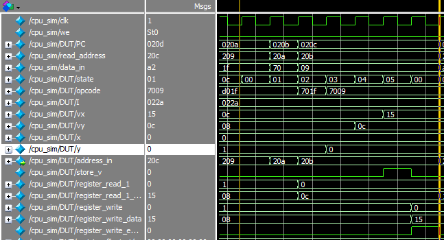
The simple instructions take 5 clocks to execute - for example the simulation output of the A239 opcode.
Example 1: A239

- request the high byte of opcode
- request low byte of opcode, store the high byte of opcode (
a2) - third clock cycle: store low byte (
39), storeVX - store
VY I := NNN- (cycle 0 of the next instruction):
Ihas the new value
Example 2: 7009
Now another instruction: 7009 - increment V0 by 9 takes 6 clock cycles:

- request high byte
- request low byte, store high byte, request value of
VX(V0) - store low byte, store
VX, request value ofVY(V0) - store
VY VX := VX + 9, raise flag that we want to storeVX- request write of
VX(V0) - (cycle 0 of the next instruction):
VXis written with the new value
Some ALU opcodes can request to store the VF flag as well.
Note: we could save one clock cycle here if the register file writes were dual-ported - we could write
VXandVFsimultaneously.
The instructions are actually implemented with a case statement within the state_execute as:
4'h1: //goto NNN
    PC <= nnn;
4'h5: // if(vx == vy)
begin
    if(vx==vy) begin
        PC <= PC + 2'd2;
    end
end
4'h7: // vx += nn
begin
    vx <= vx + nn;
    store_v <= 1'b1;
    state <= state_store_v;
end
4'hA:
    I <= nnn;
Writeback phase
This is handled by two flags for now - store_v and store_carry that indicate that we’d like to write to the register file. My current implementation uses one extra clock cycle as it just requests writeback in the execute state:
4'h6: begin // vx = nn
vx <= nn;
store_v <= 1'b1;
state <= state_store_v;
end
then doing the actual write in store_v state:
if(store_v) begin
    register_write <= x;
    register_write_data <= vx;
    register_write_enable <= 1'b1;
    store_v <= 1'b0;
end
Using Verilog task to reuse these statements could help reduce repetition if I wanted to optimize this.
Writes to memory performed by the FX33 (convert to BCD) and FX55 (store registers) opcode are handled by their separate states that will take multiple clock cycles to execute.
What’s next
To get to an useful output, I’d like to implementing the draw instruction next and wire up a VGA or LCD display to see the contents of the framebuffer. Then the rest of the instructions would be nice to implement, checking the result against a test ROM or a known working emulator